Devoid of modern improvements and technologies, prototyping and conceptual design processes are sluggish, expensive and prone to bottlenecks. This is true of just about any type of creation or development project, but even more so in regards to PCB development.
Between each build, a design must be rigorously tested and trialed — a multi-stage process that is often resource-intensive and time-consuming. If a test is outsourced, the development time is exacerbated even more simply because the design must change hands frequently.
The time it takes for complex prototypes to see approval can take weeks or even months. To make matters worse, if and when a flaw is identified, the entire process is rebooted. It may take just as long to come up with a redesign, submit it for approval again, and wait for production to start. Every single bottleneck or obstacle causes significant delays, and that’s before you even reach final production and manufacturing stages.
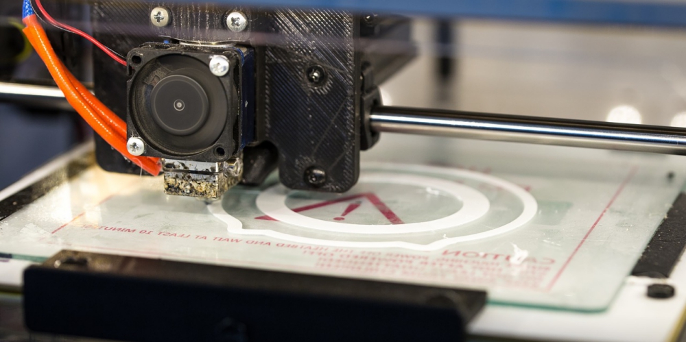
There is hope, however. 3D printing, or additive manufacturing, offers a variety of benefits, namely to conceptual and prototyping processes. A team can quickly design and print a new PCB prototype in-house and either test it internally or send it out all within the same time frame — usually the very same day. Not only does this remarkably speed up all steps of the overall process, it conserves an incredible amount of money and additional resources too.
Is Modern 3D Printing the Solution to Prototyping Woes?
The improvements of 3D printing for conceptual design sound great, in theory, but are they actually present in the real world? Does an internal additive manufacturing process actually provide benefits to a design team, particularly when it comes to the final PCB developed?
The answer is, unequivocally, yes.
One company, Nano Dimension, recently launched a 3D printer that was made for creating professional PCB prototypes. It’s called the DragonFly 2020 3D Printer and it uses inkjet deposition methods to produce objects. At its foundation is a nano-chemistry process driven by sophisticated and highly-advanced software.
The result is an incredible wealth of opportunities for PCB designers and manufacturers. Prototyping and development are shaved down to mere hours, as opposed to weeks or months. Even the most complex designs can be produced and fabricated in a matter of hours. Furthermore, the final product is almost instantly ready for testing, depending on the materials used in the printing process.
The nature of 3D printers — and how precise they work — means that designs can become infinitely more complex, adopting models and elements that never would have been possible in the past. Conductive layers and surfaces, for instance, can be printed and embedded right within the board. The creation of advanced multi-layer PCBs is also possible with modern 3D printers, simply because they develop an object by spreading layer upon layer of the composition material. Single-layer or single-sided and double-layer boards are also possible in new, innovative configurations with additive manufacturing methods.
The Change Will Not Happen Overnight
The potential of additive manufacturing in the sector is remarkable, and while a general shift in focus is coming — more and more teams will start to implement the process — it’s not something that’s going to happen overnight.
For starters, the machines themselves need to be configured and designed for conceptual creation and prototyping, much like Nano Dimension has done with their DragonFly printer. In addition, the technology must become more affordable and accessible on a commercial scale. That shift is happening, but again, it will take some time to truly make an impact across various industries.
Even so, it’s hard to deny the incredible potential that modern additive manufacturing and 3D printing technologies offer. Just the ability to print new PCBs, in-house, and dive right into testing is invaluable, let alone all the efficiency and cost benefits that come from implementing such a machine.